PCB Etching Tutorial: Difference between revisions
(add mediawiki local link for EDA) |
|||
| Line 18: | Line 18: | ||
[Insert picture of before and after here ] | [Insert picture of before and after here ] | ||
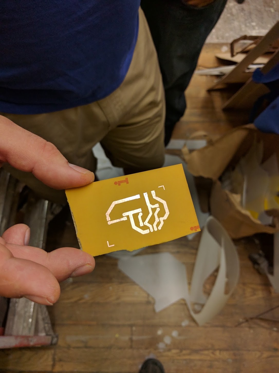
[[File:PCBetchDone.jpg]] | |||
== '''Materials Needed''' == | == '''Materials Needed''' == | ||
Revision as of 11:08, 13 September 2016
DIY PCB Etching : Using Chemicals
Chances are you've probably seen a PCB before and it might of looked a little something like this
[Insert a picture of an example of a PCB maybe a Raspberry Pi or an Arduino etc]
The most important part of a PCB is the traces which connect the components to each other. These traces made in a CAD program for PCBs like : Eagle CAD , KiCAD etc
[Insert Picture of traces here]
This tutorial will show you how to make a simple single sided PCB using a chemical method. In summary the traces will be transferred and covered in a solid copper board , then the parts of copper not needed will stay expoxed. Finally the parts not needed will be removed with chemicals.
[Insert picture of before and after here ]
Materials Needed
- Single sided copper clad board -- [[ https://www.google.com/search?q=copper+clad+fr4&ie=utf-8&oe=utf-8]]
- Circuit board trace layout in a printable format (pdf or postscript ps works, design this with an EDA program)
- Glossy Inkjet Photo Paper (to print the traces on)
- Iron or press
- Etchant chemical
- Ferric Chloride Solution (to dissolve the copper from the board)
- Muriatic Acid
- WetorDry paper
- Container to put PCB in with chemical solution
Steps
If you are using Ferric Chloride(FeCl3) foretchant, then start heating your etchant to 50C
1) Preparing the Copper Board: Clean It
Make sure to clean any junk from the copper board before beginning the process!
- Use WetorDry paper / fine sand paper to clean the PCB under water until it turns pink
- Wipe off water with a clean towel
- Use acetone to remove oils from PCB
[ insert Cleaning pics here]
2) Printing the Traces:
Grab your Laser printer and print the traces onto the glossy inkjet photo paper.
- we used walgreens 8.5x11 stock inkjet photo paper with fine results
- We used the Noisebridge Brother HL-5470DW and generic Laser printer toner with fine results
- Make sure your print driver isn't scaling or distorting the circuit layout
- Use monochrome and highest resolution possible for your printer
The printer operator should also take this opportunity to provide feedback to the circuit designer:
- Make sure the design traces are thick enough for this process (XXmil/XXmm minimum trace width with 20mil/0.508mm minimum clearance)
- Make sure the export file is mirrored. The Laser Printer toner is going to 'transfer' to the surface of the copper clad and become unmmirrored in the process
[insert printing pics here]
3) Transferring the Traces to the PCB:
  - Press down the glossy paper with the design onto the copper PCB
  - Use a hot iron to press down glossy paper to the PCB [INSERT PIC HERE OF IRON PRESSED]
  - After the glossy paper stick onto the PCB submerge the two in a tray of water and gently press down the paper so it peels off leaving the trace on the PCB
[insert PCB iron down pic here]
4) Get Rid of the remaining Copper
  - Place the Ferric Chloride Solution Bottle  inside tray of hot water (this will heat the solution and make the PCB copper to be dissolved faster)
  - Pour some of the solution into a tray along with your PCB
  - Check the PCB every 5 or so minutes to check if the copper has been fully removed
[insert PCB blood water pics here]
